PCB Development
Conventional PCB design workflows begin with discrete component prototyping on a breadboard, employing a granular setup to evaluate circuit behavior. Finalized schematics are typically derived through iterative 'trial-and-error' cycles.
Present design methodologies allow for direct translation of theoretical schematics into preliminary PCB layouts, which are incrementally optimized within ECAD environments. These platforms offer integrated simulation and verification tools, effectively replacing the need for discrete hardware testing by validating circuit integrity and performance virtually.
Despite the sophistication of simulation engines, a significant number of developers and engineers still continue to favor breadboard prototyping. This hands-on phase provides empirical data and practical insights, that inform and enhance the accuracy and robustness of the final schematic design.
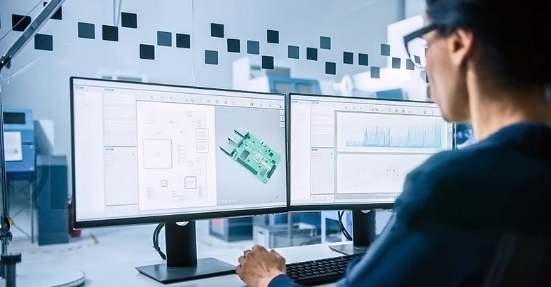
Our developers use the industry-leading Altium™ Designer, one of the most comprehensive and powerful ECAD software solutions available today. It provides all the necessary tools to achieve optimal results in the shortest development time. With its advanced simulation and management features, Altium™ Designer ensures cutting-edge outcomes in less time compared to other ECAD tools.
I’ve already created a concept design in KiCAD, UltiBoard, or MultiSIM — is that an issue? Absolutely not! We can easily convert all provided ECAD file formats and extensions into Altium™ Designer. Regardless of the ECAD suite you’ve used, we can seamlessly integrate your concept into our development workflow. Additionally, if you'd prefer to continue working within your own ECAD environment, we can convert Altium™ Designer files back to your preferred format without any trouble.
Today's Printed Circuit Boards have come a long way. The evolution of PCBs has driven such innovation that circuit boards are now found in everything, from basic electronics in children's toys to sophisticated, high-end smartphones. However, these circuit boards don't just appear out of nowhere. Before production of the final product begins, there is a comprehensive PCB development process, and it often involves several delays along the way.
The Complete Electronics Design Process
█ 1. Requirements Definition
█ 2. Estimates
█ 3. Design Proposal - Cost and Timescales
█ 4. Project Plan
█ 5. Design Specifications
█ 6. Schematic Design
█ 7. PCB Design
█ 8. Prototype Manufacturing
█ 9. Environmental Testing
█ 10. Setup of Production Manual and BOM
█ 11. Production Management
Once the electronic schematic has been fully defined and all design revisions have been locked in, the PCB layout phase commences. Leveraging Altium™ Designer, our engineers can run pre-layout and post-layout simulations, as well as perform comprehensive design rule checks (DRCs) and electrical rule checks (ERCs), ensuring design integrity and identifying potential signal integrity or power distribution issues early on.
These iterative validations not only minimize the risk of downstream failures but also enable targeted optimizations that enhance overall system reliability. Despite these precautions, it’s essential to recognize that the initial hardware build—commonly referred to as the Proto-0 board—functions primarily as a proof-of-concept and may exhibit unforeseen performance issues or design limitations requiring further iteration.
Once the first version of the PCB is manufactured, error-free operation is not guaranteed. Before deploying a fully functional prototype (Proto-0), it’s essential to thoroughly test the PCB and identify any bugs or issues that may arise.
At this stage, it’s common to encounter bugs within the microprocessor (µProcessor) or microcontrollers (µControllers) that need to be resolved. The Microcontroller Unit (MCU), working in conjunction with the embedded µProcessor, acts as the "digital traffic controller" of the electronic device—managing critical components such as memory, sensors, actuators, displays, and switches. When issues are identified in the µController, it must be reprogrammed.
Our developers use Visual Studio Code with compilers for C, C++, or C# (C-sharp), or alternatively CodeFusion Studio™ when working within an embedded software environment, to write and refine the code for both the µProcessor and µController. This cycle of debugging, testing and evaluating changes may need to be repeated multiple times to achieve the desired functionality—ensuring the system not only performs correctly but also maintains stable operation.
After the PCB undergoes comprehensive functional testing, the design team assesses its compliance with the specific requirements for the intended device. Unlike the broader product development cycle, where the PCB is just one component, this phase is dedicated to ensuring that the board integrates seamlessly into the overall product. This includes both mechanical and electrical compatibility.
In close collaboration with developers and mechanical engineers, any necessary adjustments are identified, ensuring that all components, from connectors to power distribution, interact flawlessly and function as a cohesive system. This step ensures that the PCB not only performs electrically but also fits perfectly within the mechanical constraints of the product design.
Mechanical-electrical integration begins with adapting the PCB layout for its target enclosure, ensuring alignment with mechanical constraints and interface points. The cross-disciplinary team—comprising mechanical engineers, industrial designers and electronics developers—validates the board's functionality & compliance with all electrical and mechanical specifications after iterative revisions.
Once verified, mechanical parameters such as mounting points, clearances and connector positioning are fine-tuned for optimal enclosure fit. Subsequently, critical factors like mechanical stress, vibration resilience, and thermal distribution are analyzed through finite element simulations and real-world testing, ensuring reliable heat dissipation and long-term system stability.
More Specifics...
The full scope of PCB development for high-end audio and automation systems goes far beyond what we can explain on a single page. These designs often involve complex multilayer layouts, precise mixed-signal routing, careful power distribution, and stringent EMI control — all critical for maintaining audio fidelity and system stability. If you're interested in how we approach professional-grade hardware design, or want to discuss specific technical aspects, feel free to reach out by phone or email.
Abilities driving results
A review of project outcomes and supporting data shows that 92% of our projects met the agreed development timeline—a steady improvement from previous years. This progress is the result of ongoing enhancements to our workflows, proactive risk management and improved team coordination. We remain committed to refining our approach to ensure your product is delivered reliably and on schedule.